onsdag 22 februari 2017

The prodigy #10 - the BCD display part 4

Now when the segments works we need to select the right digit to lit. MAME has a layout system where it is possible to create simple layouts from textual descriptions. We will create a small layout and show how to manipulate this from the driver. The BCD digit is defined like this:
<led7seg> <color blue="0.0" green="0.0" red="0.75"></color>
</led7seg>

Which allows us to make it redish. The actual BCD display should look something like the picture to the right. To actually place out some digits we use the bezel
<bezel element="digit" name="digit0">
<bounds bottom="885" left="70" right="100" top="840">
</bounds>
This defines "digit0" which can be manipulated from the driver by including the layout, or rather the compiled version which is compressed during build time.

#include "prodigy.lh"


We need to synchronize the update of the UI digit element with the ROM software so we know when to present the segments and to which digit. Fortunately there is an interrupt firing between the VIA shift register updates so we can create yes another trampoline in the driver code for this

MCFG_VIA6522_IRQ_HANDLER(WRITELINE(prodigy_state, irq_handler));

This handler is now responsible for interrupting the CPU but we also do the update of the BCD display

WRITE_LINE_MEMBER(prodigy_state::irq_handler)
{
    m_maincpu->set_input_line(M6502_IRQ_LINE, state);
    update_bcd();
}


We need also to know which digit to lit so we need to feed the 74145 from the VIA Port B bit 0 and 1. In fact Bit 2 and 3 are also connected but used for something else that we will explore later.

MCFG_VIA6522_WRITEPB_HANDLER(WRITE8(prodigy_state, via_pb_w))
...
WRITE8_MEMBER( prodigy_state::via_pb_w )
{
    m_74145->write( data & 0x0f ); // Write PB0-PB3 to the 74145
}

Viola, so when the interrupt fires the 74145 can be read to know the digit:

void prodigy_state::update_bcd()
{
 LOGBCD("%s\n", FUNCNAME);
 uint8_t ttl74145_data;
 uint8_t digit_nbr = 4;

 ttl74145_data = m_74145->read();

 if ((ttl74145_data & 0x0f) != 0x00)
 {
  switch (ttl74145_data & 0x0f)
  {
  case 0x01: digit_nbr = 0; break;
  case 0x02: digit_nbr = 1; break;
  case 0x04: digit_nbr = 2; break;
  case 0x08: digit_nbr = 3; break;
  }

  m_segments = m_digit;
  output().set_digit_value( digit_nbr, m_segments);
 }
}

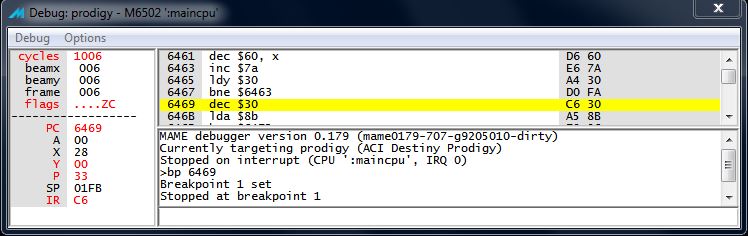
The last statement will form the tag = "digit%c", '0' + digit_number; eg digit0 to digit3, and then lit the segments for that digit in the layout. Running the final code will render this in MAME:


Next step will be to trace out the keypad and get the software running, stay tuned!

tisdag 21 februari 2017

The prodigy #9 - the BCD display part 3


Netlist is a CPU device in MAME that slices the time at a higher rate than the clocks on the other devices and is because of this able to calculate levels in analog as well as in digital circuits between the clock cycles. This is important as it can also span multiple clock domains and synchronize independently running sub circuits including CPU:s.

The drawback is of course that it takes more host CPU power to emulate things this way so the trick is to find a good mid ground. In the prodigy project we need a 74164 device that is implemented as part of the Netlist framework in order to contribute to this better emulation.

In the previous blog we checked out how to emulate the 74164 the usual way. To do the same thing using MAME Netlists we need to write a netlist device and it is also quite small however the way of connecting it the Prodigy driver is more complex.

If we start with the device configuration it looks like this:

MCFG_DEVICE_ADD(NETLIST_TAG, NETLIST_CPU, XTAL_2MHz * 30)
MCFG_NETLIST_SETUP(prodigy)

MCFG_NETLIST_LOGIC_INPUT(NETLIST_TAG, "cb1", "cb1.IN", 0)
MCFG_NETLIST_LOGIC_INPUT(NETLIST_TAG, "cb2", "cb2.IN", 0)
MCFG_NETLIST_LOGIC_OUTPUT(NETLIST_TAG, "bcd_bit0",  "bcd_bit0",  prodigy_state, bcd_bit0_cb, "")
MCFG_NETLIST_LOGIC_OUTPUT(NETLIST_TAG, "bcd_bit1",  "bcd_bit1",  prodigy_state, bcd_bit1_cb, "")
MCFG_NETLIST_LOGIC_OUTPUT(NETLIST_TAG, "bcd_bit2",  "bcd_bit2",  prodigy_state, bcd_bit2_cb, "")
MCFG_NETLIST_LOGIC_OUTPUT(NETLIST_TAG, "bcd_bit3",  "bcd_bit3",  prodigy_state, bcd_bit3_cb, "")
MCFG_NETLIST_LOGIC_OUTPUT(NETLIST_TAG, "bcd_bit4",  "bcd_bit4",  prodigy_state, bcd_bit4_cb, "")
MCFG_NETLIST_LOGIC_OUTPUT(NETLIST_TAG, "bcd_bit5",  "bcd_bit5",  prodigy_state, bcd_bit5_cb, "")
MCFG_NETLIST_LOGIC_OUTPUT(NETLIST_TAG, "bcd_bit6",  "bcd_bit6",  prodigy_state, bcd_bit6_cb, "")
MCFG_NETLIST_LOGIC_OUTPUT(NETLIST_TAG, "bcd_bit7",  "bcd_bit7",  prodigy_state, bcd_bit7_cb, "")

As can be seen the NETLIST_CPU runs at 30 times the 2MHz of the CPU and VIA devices. This is not a tuned value at this point as we may need to add more things ot the Netlist later. The second thing that strikes the eye is that there is no sign of the 74164 itself but instead a netlist called 'prodigy'. This is because the circuit itself is a sub device put in separate file, the setup of the 74164 looks like this:

 TTL_INPUT(cb1, 0)
 TTL_INPUT(cb2, 0)

 TTL_74164(SHIFT, cb2, cb2, high, cb1)
 ALIAS(bcd_bit0, SHIFT.QA)
 ALIAS(bcd_bit1, SHIFT.QB)
 ALIAS(bcd_bit2, SHIFT.QC)
 ALIAS(bcd_bit3, SHIFT.QD)
 ALIAS(bcd_bit4, SHIFT.QE)
 ALIAS(bcd_bit5, SHIFT.QF)
 ALIAS(bcd_bit6, SHIFT.QG)
 ALIAS(bcd_bit7, SHIFT.QH)


To actually hook up all this to the VIA requires some more glue, first we need to tell MAME that we need the netlist circuit and the inputs to it.


 required_device<netlist_mame_device_t> m_bcd;
 required_device<netlist_mame_logic_input_t> m_cb1;
 required_device<netlist_mame_logic_input_t> m_cb2;


We also the callbacks where the Netlist communicates back the changes in signal states:


NETDEV_LOGIC_CALLBACK_MEMBER(prodigy_state::bcd_bit0_cb) 
{ 
 if (data != 0) 
  m_digit |= 0x01;
 else 
  m_digit &= ~(0x01);
}

Lastly we use some trampoline methods to route the VIA output into our Netlist:


MCFG_VIA6522_CB1_HANDLER(WRITELINE(prodigy_state, via_cb1_w))
MCFG_VIA6522_CB2_HANDLER(WRITELINE(prodigy_state, via_cb2_w))

WRITE_LINE_MEMBER(prodigy_state::via_cb1_w)
{
 LOGCLK("%s: %d\n", FUNCNAME, state);
 m_cb1->write(state);
}

WRITE_LINE_MEMBER(prodigy_state::via_cb2_w)
{
 LOGCLK("%s: %d\n", FUNCNAME, state);
 m_cb2->write(state);
}

To summarize the chain of events that takes place:

  • The CB1 and CB2 trampoline handlers, via_cb1_w and via_cb2_w respectivelly, are called when the VIA device generates changes on these outputs. 
  • The  handlers calls the write method on the netlist input devices m_cb1 and m_cb2. 
  • The netlist is crunched at 30 times the CPU clock, at an emulated 60MHz, and are able to calculate the logical signals at this rate. 
  • When the 74164 output signals enters a TTL low or high levels the bcd_bitx_cb() callback routine corresponding to the bit that has changed is called with the logical state. 
  • The callbacks finally compiles all the changes into a 8 bit pattern which are the segment values to be lit!
Next thing is to lit the correct BCD display! 

The prodigy #8 - the BCD display part 2

In order to emulate the Prodigy BCD display we need to write a 74164 device as MAME currently not has it. This should be straight forward as the chip is quite simple.


In MAME there are plenty of devices already emulated that can be configured and connected to other devices in a specific board driver using some MCFG macros. The MCFG macros are a loosely standardized way of configure and setting up relationships between devices in MAME.

To connect devices to the executed ROM code these are either mapped onto the address map using AM macros where a specific function in the device driver is called when accessing the address range. Which one however varies from device to device and you need to study how other have done it or just read the device source code.

In our case the 74164 is connected through the VIA device which we mapped up earlier using the following lines of macros:

MCFG_VIA6522_CB1_HANDLER(DEVWRITELINE("shift", ttl74164_device, a_w)) 
MCFG_VIA6522_CB2_HANDLER(DEVWRITELINE("shift", ttl74164_device, clock_w))
MCFG_74164_ADD("shift")

These macros connects the newly written device 'ttl74164_device' instance called 'shift' with clock input from VIA CB2 output and the A input from the VIA CB1 output. Last rows adds the actual 74164 itself and names it "shift" so MAME can look it up in runtime when putting the pieces together.

Now the missing piece is the 74164 driver itself. I wrote it up the classical way and submitted a PR to MAME, check it out here, but it was rejected as will all synchronous devices going forward. Here is why:

The way MAME works each CPU gets a certain amount of time to execute. When accessing devices the state of the signals are always adjusted according to the input in a chained manner which works pretty well as long as there is only one CPU/device talking. As soon as there is another source of changes such as a clocked circuitry there is a risk that the one part of the circuit is not up to date with the other clock.

This was revealed in a parallel work in MAME by Ryan Holtz with the Hazeltine driver, where multiple devices were supposed to deliver a unified bit field on an edge of a clock and in fact only the first part of the circuit held the expected data at the time as the latter part had not yet been updated. This is a common problem with logic emulation in general why there is a technique using oversampling so that sub cycle changes can be emulated at a higher precision than just connecting the signals.

This is accomplished in MAME by using the Netlist CPU contributed by Couriersud. It is not a traditional CPU but a device that runs at a higher clock rate than the emulated clocks in the system and constantly updates a circuit described as a Netlist This is what is used in the Pong game MAME emulation.


The Pong game had no CPU but only discrete components. The MAME Netlist system can describe both analog and logic circuits even mixed together at a decent performance.

Lets see how we can use a Netlist to solve the multiple clock alignment problem in MAME for the 74164 next!

The prodigy #7 - the BCD display part 1


Tracing the VIA towards the BCD display revealed an interesting circuit to emulate. The 6522 VIA has a poor mans UART builtin in the form of a 8 bit shift register that is very versatile. It can shift both in and out clocked by internal timers, the VIA clock or an external clock. It also has a continuous mode so all together there are numerous ways to use it. In the prodigy it is used to drive the segments of the BCD display.


The BCD display is of common anode type where two bits on VIA port B selects one of the four anodes to light up through a TTL 74145 chip. The shift register is set up by the Prodigy ROM to put the internal VIA clock on CB1 and data on CB2 which is connected to a 74164 chip which translates the bits shifted in to it to an 8 bit output which drives the segments for one of the 4 BCD displays selected by the 74145. There is a need for more current than the TTL circuits can drive to lit up the segments and why there is also 4 x PN2907 transistors and 2 x 75491 chips to boost the current.

Now, how would we emulate this in MAME? First we need to check what chips are already emulated and a quick check in the source code repository reveals that there was no 74164 device.

So the next thing to do is writing a 74164 device and add that to MAME.

torsdag 1 december 2016

The Prodigy #6 - Document the PCB layout

An important step in the preservation work is to document the PCB not only as images but also as part of the emulation source code so that later maintainers easily can see what circuit design is being emulated. It can reveal inexact emulation and also help determine the revision of a future PCBs that is up for preservation.

Using mono spaced text for the layout has its limitation but the important thing is to be able to see the resemblance  with the real thing. We start with the PCB edges, add connectors and the large chips and continue with the smaller ones and try to be at most 120-150 characters wide.

Some examples of ascii layout components
The ascii layout goes directly in to the source code together with whatever chip references there are and of course also links to the original images if they are public such as our Prodigy page

To get the right start I usually start in Gimp or Power Point where I put the original image and a half transparent text layer on top of it choosing a small mono spaced font such as Courier New of size 8-12 depending in the size of the board. Gimp and Power Point are pretty poor editors so once I have some reference points I copy all of the text into good old Emacs and finalize the work there.

Layout outline copied from half transparent text layer in Power Point
So to compare this with the top PCB image


you see that it is pretty easy to find the right chip when referring it from the source code. From here it is just to fill in the missing parts and we have given the future maintainer and computer archaeologist quite a few hints about what this design looked like.

Back in Emacs I will at this point turn on the overwrite mode, by pressing the Ins key, so I freely can add characters at any point in the layout without shifting the ones right of the cursor further to the right. To make it even easier it helps to fill out the width of the layout with spaces so the cursor doesn't flung left when it comes to a shorter row.

When editing the last details it is very useful to have the image visible at the same time as the editor so by enabling the truncate-long-lines option in Emacs it is possible to place the windows side by side

Editing the ascii layout

The final version is adjusted and made complete for reference.
Final ascii layout

This is a good picture to refer to from the code we are about to write, check it out on github.

Next we continue to trace down the VIA ports

torsdag 24 november 2016

LaserWriter II NT

I am writing an emulator for this board in order to support Localtalk for the MAME. The information on Internet reveals enough to get started and I also got hold of a romset. The whole CPU power is located on what they consider an I/O board but it really does all the rendering of Postscript and emulation of the old Diablo 630 daisy wheel protocol.

I found some pictures here that I stitched together:


As can be seen there was a few areas missing at the bottom of the PCB but it is really helpful when trying to trace board. Unfortunately the board is one of the first revs using a TPI6523 while the romset has been proven to use the newer VIA6522 chip, the same as used in the Commodore 64 btw :)

Obviously the pcb has more than two layers as the connectors to the left, unfortunately not pictures as the front panel covered that part of the pcb, has no visible traces and there are in-penetrable areas of copper on both sides in that area

fredag 18 november 2016

The Prodigy #5 - add a timer interrupt

After "properly" hooking up a VIA device the next thing we want is to see how the ROM is programming it. As we now have hooked the VIA up properly there will be no warnings on the MAME debugger console (Ctl-L remember?) But this can also be achieved by using watch points in the MAME debugger, like

wp 0x2000,f,w

and then just hitting F5 a couple of times when the watch point triggers, or as in my case, temporary instrument the VIA driver with some proper printouts. Then it is just to decode the bytes written to see what it is up to:


This reveals a lot how the PCB are designed but for now we are just interested in the interrupts as the code seems to be waiting in a tight loop for something to end up in the RAM area, most probably delivered by an interrupt. The last line gives us a clue what interrupt that might be, the Timer 2 interrupt is enabled, we just need to hook it up to the CPU and see where it takes us.


By pressing F7 in the MAME debugger it will execute the ROM until an interrupt happens, and indeed it stops immediately


0x79F8 is indeed the right vector. Now if we set a breakpoint after the tight loop we identified prior enabling the interrupts, let's see what happens.


Hmm, it doesn't trigger. Lets fake input via the RAM location at 0x30 through the memory window (Ctl-M)

Click at the low nibble of the memory location first because the high seems reset all bits set faster than the editor can zero them, and voila!


It obviously hits the bp but more important is that the interrupt routine seems fiddling with the 0x30 as well. Next step is to examine the interrupt routine and discover the port usage, mañana! Next->