torsdag 1 december 2016

The Prodigy #6 - Document the PCB layout

An important step in the preservation work is to document the PCB not only as images but also as part of the emulation source code so that later maintainers easily can see what circuit design is being emulated. It can reveal inexact emulation and also help determine the revision of a future PCBs that is up for preservation.

Using mono spaced text for the layout has its limitation but the important thing is to be able to see the resemblance  with the real thing. We start with the PCB edges, add connectors and the large chips and continue with the smaller ones and try to be at most 120-150 characters wide.

Some examples of ascii layout components
The ascii layout goes directly in to the source code together with whatever chip references there are and of course also links to the original images if they are public such as our Prodigy page

To get the right start I usually start in Gimp or Power Point where I put the original image and a half transparent text layer on top of it choosing a small mono spaced font such as Courier New of size 8-12 depending in the size of the board. Gimp and Power Point are pretty poor editors so once I have some reference points I copy all of the text into good old Emacs and finalize the work there.

Layout outline copied from half transparent text layer in Power Point
So to compare this with the top PCB image


you see that it is pretty easy to find the right chip when referring it from the source code. From here it is just to fill in the missing parts and we have given the future maintainer and computer archaeologist quite a few hints about what this design looked like.

Back in Emacs I will at this point turn on the overwrite mode, by pressing the Ins key, so I freely can add characters at any point in the layout without shifting the ones right of the cursor further to the right. To make it even easier it helps to fill out the width of the layout with spaces so the cursor doesn't flung left when it comes to a shorter row.

When editing the last details it is very useful to have the image visible at the same time as the editor so by enabling the truncate-long-lines option in Emacs it is possible to place the windows side by side

Editing the ascii layout

The final version is adjusted and made complete for reference.
Final ascii layout

This is a good picture to refer to from the code we are about to write, check it out on github.

Next we continue to trace down the VIA ports

torsdag 24 november 2016

LaserWriter II NT

I am writing an emulator for this board in order to support Localtalk for the MAME. The information on Internet reveals enough to get started and I also got hold of a romset. The whole CPU power is located on what they consider an I/O board but it really does all the rendering of Postscript and emulation of the old Diablo 630 daisy wheel protocol.

I found some pictures here that I stitched together:


As can be seen there was a few areas missing at the bottom of the PCB but it is really helpful when trying to trace board. Unfortunately the board is one of the first revs using a TPI6523 while the romset has been proven to use the newer VIA6522 chip, the same as used in the Commodore 64 btw :)

Obviously the pcb has more than two layers as the connectors to the left, unfortunately not pictures as the front panel covered that part of the pcb, has no visible traces and there are in-penetrable areas of copper on both sides in that area

fredag 18 november 2016

The Prodigy #5 - add a timer interrupt

After "properly" hooking up a VIA device the next thing we want is to see how the ROM is programming it. As we now have hooked the VIA up properly there will be no warnings on the MAME debugger console (Ctl-L remember?) But this can also be achieved by using watch points in the MAME debugger, like

wp 0x2000,f,w

and then just hitting F5 a couple of times when the watch point triggers, or as in my case, temporary instrument the VIA driver with some proper printouts. Then it is just to decode the bytes written to see what it is up to:


This reveals a lot how the PCB are designed but for now we are just interested in the interrupts as the code seems to be waiting in a tight loop for something to end up in the RAM area, most probably delivered by an interrupt. The last line gives us a clue what interrupt that might be, the Timer 2 interrupt is enabled, we just need to hook it up to the CPU and see where it takes us.


By pressing F7 in the MAME debugger it will execute the ROM until an interrupt happens, and indeed it stops immediately


0x79F8 is indeed the right vector. Now if we set a breakpoint after the tight loop we identified prior enabling the interrupts, let's see what happens.


Hmm, it doesn't trigger. Lets fake input via the RAM location at 0x30 through the memory window (Ctl-M)

Click at the low nibble of the memory location first because the high seems reset all bits set faster than the editor can zero them, and voila!


It obviously hits the bp but more important is that the interrupt routine seems fiddling with the 0x30 as well. Next step is to examine the interrupt routine and discover the port usage, mañana! Next->


The Prodigy #4 - add some RAM and a VIA device

The latest findings in the effort to preserve and emulate the Prodigy reveals that we need to move ROM to address 0x6000 and add some RAM. The easiest way to allow something on both 0x6000 for execution and 0xe000 in order to provide a reset vector from 0xFFFC is simply to ignore address lane A15 such that the ROM is selected in both places. No circuits I have seen on the PCB so far tells me that we have a more advanced decoding so lets ignore A15!

In MAME this is done using the AM_MIRROR macro with an argument that tells MAME what lanes to ignore for this particular device, in our case the argument is 0x8000 as we want to ignore A15. Adding some RAM at 0x0000 is simple, the M58725P is a 2KB so the range is between 0x0000 and 0x07ff:


So lets fire up the MAME debugger again and see where we end up:


Hiya, the PC after reset point at the address 0x60B7, just like we wanted! :) All good so far. Lets what we miss in our address map by opening the console (Ctl-L) and run the code (F5).


Interesting, there are just a few accesses to the VIA at startup and then the CPU lies in a tight loop waiting for address 0x30 to change while stepping up address 0x7A. This suggests that the VIA will change address 0x30 using interrupts, unless the VIA is very strangely mapped to these addresses directly! Lets hook it up and see what happens.

Add the definitions of the VIA driver

Initiate the instantiated VIA device called m_via
Tell MAME that this is a required device, not a lot option or otherwise optional in any way 


Map the device to the address space we have identified

Add the device to the machine, lets use the CPU 2MHz crystal for now

Don't worry I have submitted this skeleton driver to Github so you don't need to stitch it together yourself and figure where they end up in the driver. These steps are the minimum when adding a new device. In addition we need to configure drivers for the interrupt and what will happen when the ports are accessed, but that is for later, c ya! Next-->

The Prodigy #3 - make a ROM adapter

Well, the cheap ass adapter to get the R2912 ROM read involved a manual step to reassemble the ROM in which case I may have done it wrong and hunting ghost bugs afterwards. In any case when I saw the image to the left below I decided to go for the correct adapter and read out the R2912 as a 2764.


This worked out beautifully and we can now establish that the Rockwell R2912 is pin compatible with a 2364 mask programmable ROM. I wonder about the R2907 still but that's not our problem at the moment. :)

In order to fit the new ROM file into the MAME driver we need the following adjustments to the code:


We start at 0xe000 as rom now is 8KB or 0x2000 bytes in hex so the reset vector is at 0xFFFC. We also need to enlarge the size of "roms" region to 0x2000 and update the size of the rom to 0x2000. The offset where we load the rom within the "roms" section is still 0x0000 though.

Firing up MAME again we see that the reset vector now seems to be 0x60B7 which is within the identified actual ROM area. Since we mapped the "roms" at the top we end up in nowhere:


By setting the PC to 0xE0B7 we can observe and step though the actual code as long as it is position independent:

Now we end up in real code and it does stuff that will tell us more about the system. We can see that the code store things at 0xAB and 0x2003. The latter look very much like a device address which usually is decoded at a nice even address boundary such as 0x2000. This means the RAM is mapped at 0x0000.

So I will map some RAM at 0x0000 and the VIA at 0x2000 next, stay tuned Next -->

torsdag 17 november 2016

The Prodigy #2 - identify the ROM type

Once we have some ROM code to work with it is time to take a look at it in action. I do that by writing a minimal skeleton driver for the MAME emulator:


The driver is just assuming that the CPU is a 6502 and that the 2KB ROM is mapped at he highest possible adresses as the reset vector must be in the ROM area. No RAM or other devices are assumed at this point as they can be easily added later when we know more.

This allows me to open up the ROM:s in the MAME debugger and start looking around. First I look at the reset vector to see where the entry point is:


Disappointingly the reset vector at adress 0xFFFC and 0xFFFD is very wrong! :(

It points at 0x0111 which is a quite unlikely remapping of the ROM. Either ROM is trashed, I didn't read it correctly or both. Even if it is mapped somewhere else the reset vector must be mapped to these addresses at power up reset. We can check this by review the disassembly view


The first observation scrolling through the code is that is seems ok, no strange trashed areas or so.

Now we look for absolute jumps which to some degree of certainty will reveal some addresses of ROM code. It does, but now the second important finding is that the jumps are more than 2KB apart, eg JSR $6580 on address $FB7A and JMP $749D on address $FB7F.

This tells us two things, the ROM executes in the $6000 range upwards probably towards the $7FFF mark which should be an 8KB ROM! I errornously assumed that 8KB didn't fit in a 24 pin DIP package but I vaguely remembered a device called 2364 and indeed a search away I found a data sheet and an instructable how to make some 2364-27xx adapters.

So I think I'll go for the 'cheap-ass' adapter and wish the Prodigy ROM is not clocked, hiya! Next-->

The preservation of the Prodigy Chess computer


I really like chess computers but usually they are too integrated to easily preserve so they kind of piled up in the garage: A Boris Diplomat, already preserved by Sean Riddle, a Mephisto Mini and a Mephisto Tutor among others. However this time I bid for an ACI Destiny Prodigy and got it!

The first thing to do in order to preserve an old MCU design is to check if anyone has done it before or if there are pictures of the inside already. I found plenty of information of this classic but no emulation in MAME or elsewhere easily found. Great, lets do it!

Among all the information on the net I found pictures of the PCB revealing it has a very discrete design, that is it uses a 6502 with external RAM and ROM chips that are easily accessible. So carefully I opened the chess computer revealing the PCB. Here I stumbled on the first issues, the RAM and ROM were not of brands I already knew:

The RAM is a Mitsubishi M58725P which I didn't recognize but a quick Google revealed that it is pin compatible with a standard 6116 2KB static RAM. So far so good. The ROM however, a Rockwell R2912, has no information easily available on Internet. The chess sites mentions that the ROM is 8KB but that would require more pins than the 24 shown in the pictures. I also saw that the pictures showed a R2907 so the information can refer to 8Kbit aka 1KB x 8 bits. EDIT: But didn't!

Interestingly enough the PCB from the net had other RAM and ROM brand, so my PCB was clearly a newer revision than the pictured one found on the Internet. Since I had no data sheet available the next step is to follow the traces and see if I can figure out what they are. This is done by a simple beeper:

I verified that all the pins were connected to the data or address bus according to the 24 pin 2716, which was my suspect and they were except for pin 18 (*OE), 20(*CE) and 21(VPP). Now the only danger I could think of was if the device required negative voltage which my ROM reader doesn't supply and which also in some cases are very destructive for the device if not supplied according to the datasheet.

I was looking carefully for circuits that could generate a negative voltage from batteries but none were found if it was even possible at the time to a cost suitable for a consumer grade product. I didn't think so and put the ROM into the ROM reader which happily read the ROM as a 2716!

Now starts the work of figuring out the inner secrets of the Prodigy hidden in the PCB and revealed by the ROM code. I will collect all info I find on my Prodigy page, stay tuned! Next-->

fredag 7 oktober 2016

MAME: Donated hardware for dumping

I got two PCB:s in the mail donated by Robert Quenet who is building emulator cabinets out of some old fruit machines.


Since I think the old fruit machines are worth preserving I dumped the roms and put up one page each to collect the information for later use.

The one at left was made 1993 by Fun Tech and based on a Z8400 processor and has 4 roms. While dumping one of the roms were sitting tight and the top broke off, either because the chip was old and had a crack or because I was a bit too eager. When I read out the content of the rom the reader told me a checksum that was different form what the label at the top said which worried me a bit, but soon later it has been verified that the rom was ok, only of the wrong size hence the checksum was wrong.

The one at the right was made around 1997/98 by Subsino and had only custom labels on the chips, however this brand is well known and there are drivers in MAME already which may fit the roms.

Just a day or so after I published the dumps I got the first results from Haze who had tinkered a bit with the Funtech roms and found that they fit well into one of two different drivers already in MAME too. He quickly produced the following screens from the roms:


Sooner or later these old fruit machine may be playable by people again without loosing loads of money and we all remember them from pubs and casinos end of the previous millennia!
Update: Early binary of the MAME emulation is here

tisdag 4 oktober 2016

MAME: Ironing out the address map from schematics

The other day I was very lucky, I got the schematics sent to me from Kron Ltd in Ukraine, for a thing I bought on the Ebay a year ago or so. The thing is a Kron K-180, a Z180 based terminal server from the mid 90:ies made up of east block TTL equivalent chips with Cyrillic characters! See my Kron180 page  for all the details.

When you got the schematics it can be quite easy to extract the address map. In this case we can see that the entire address space is divided into two parts by enabling the ROM when A15 is low and the RAM when it is high. We can also see that the A14 and A13 is not attached on the RAM chip since there is only 8Kb of RAM. This is how I present this to MAME:


The AM_REGION and AM_SHARE creates labels that I can use when loading the ROM and mapping the screen memory onto the emulated video device. The AM_MIRROR says that the A13 and A14 is not used when the range is selected hence it will be mirrored on the upper 24Kb om memory map. ADDRESS_UNMAP_HIGH simply says that unmapped areas are read as 0xFF.

The Zilog and other Intel like CPU:s also has an IO map, which Motorola like CPU.s doesn't. The IO map is selected when the special instructions IN and OUT are used and involves its own bus control signalling. Here the schematics are not as simple as for the RAM and ROM.

There are two decoder chips on the K-180 pcb that decides what device will be accessed and how, the first is the standard decoder chip 74138 and then there is a cascaded 74259 latch. They are hooked up like this:
74138
74259

As can be seen we now have all the address lines A0 to A7 defined. With a bit of tracing we can see that the Q0 output of the 138 is connected to the 259 at pin 14 which is active low. There is also A7 connected to pin 4 at the 138, active low. An interesting detail is that A3 is connected as data input to the 259 which means that there are different output level on O0-O7 accessing the 259 in IO range $00-$0F compared to $40-$4F and it is also locked until the next access.

The 138 is only active low during the access cycle itself. With all this information it is quite simple to trace the schematics and see what signals and devices are accessed for the Q1-Q7 outputs of the 138 and the O0-O7 output of the 74259.

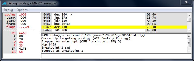
Now, the Z180 has internal I/O registers between $0 and $3f which happens to overlap with the identified adress map, unless it is relocated. This can be done by setting the ICR register and by setting an IO access breakpoint at the ICR register in the MAME debugger we can easily verify that the internal registers are relocated to $80-$BF


74299
As a working assumption we model all accesses as writes just setting and pulse signals, except for 74299 which has an easily spotted parallel output that is connected to the data bus:

Then we can setup the complete IO map in our driver like this:


We handle the 259 latches as a single item since there are hidden data in the address. In order to debug this I declare stub functions in the K-180 board driver:


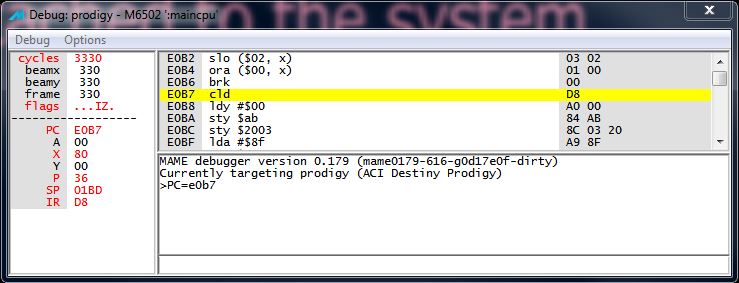
As can be seen there are special cases when accessing the 259 and also when reading from the 299. By setting a watch point in the MAME debugger we can verify that the assumptions are correct


Hmm, there are reads from offset $10 which is mapped to the AP5 line, interesting!

Checking out the schematics again we can see that AP5 is chip enable on another 74299 and that the writes to $F and $7 toggles the clock to the EEPROM. A not so wild guess is that the second 74299 is used to read out the EEPROM.

So I add another stub for reads at offset $10 and continue to go through the startup code as far as the code executes without crashing or misbahaving. When it does I need to go back and add real code to the stubs and reiterate the process until all devices in the IO map are identified.

Then the fun starts, stay tuned!